Rewriting the rules: Huawei’s new gamble to break the US’s chip blockade
Huawei has unveiled a new chip design law that could help China bypass US semiconductor restrictions and achieve tech sovereignty. Lianhe Zaobao associate editor Han Yong Hong tells us more.
29 May 2026
Technology
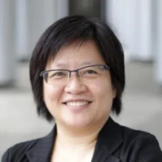

On 25 May, He Tingbo, president of Huawei’s semiconductor business department, set China’s public discourse and semiconductor industry abuzz with her address at an event in Shanghai.
Homegrown expert’s breakthrough
At the IEEE International Symposium on Circuits and Systems, He unveiled the Tau Scaling Law in her keynote speech, along with a paper published in her name. She explained that by reducing the time constant, or tau, through its LogicFolding technology, Huawei has successfully designed and mass-produced 381 chips over the past six years.
She predicted that by 2031, the high-end chips Huawei designs based on the Tau Scaling Law are expected to feature a transistor density that is equivalent to 1.4-nanometre processes. In other words, Huawei would be able to bypass US restrictions and manufacture more advanced chips.
The 57-year-old He, a native of Changsha in Hunan province, holds a master’s degree in communications engineering and semiconductor physics from Beijing University of Posts and Telecommunications. She joined Huawei at the age of 27 and has remained there ever since, making her a semiconductor expert trained entirely within China.

To use an old self-deprecating Chinese expression, researchers with such backgrounds were once referred to as “tubie” (土鳖, lit. “local bumpkins”), in contrast to “haigui” (海龟, “sea turtles”), a term for those who studied abroad and later returned to China. However, with the emergence in recent years of outstanding homegrown talent in fields such as robotics and artificial intelligence, “tubie” has largely lost its negative connotation. It is said that the team behind DeepSeek founder Liang Wenfeng is also composed largely of graduates from Chinese universities.
He previously served as president of HiSilicon, Huawei’s semiconductor subsidiary. Beginning in 2004, she led efforts to independently develop chips for consumer electronics products. At the time, Huawei founder Ren Zhengfei made a major commitment to the project, allocating the then 35-year-old He a team of 20,000 people and an annual research and development budget of US$400 million, in the hope of achieving a breakthrough in self-developed chips.
For many years, however, the team remained as a “spare tyre” within Huawei. That changed in 2019, when the administration of then US President Donald Trump placed Huawei on the Entity List on national security grounds. The move barred American companies, as well as foreign firms using US technology, from exporting semiconductor hardware and software to Huawei. Washington also pressured the Netherlands not to export extreme ultraviolet (EUV) lithography machines to China — equipment essential for manufacturing advanced chips.
Engineering optimisation
In May that year, He wrote an open letter to HiSilicon employees announcing that the “spare tyre” team she had led for more than a decade had become the main force overnight. The passionate internal letter went viral on Chinese social media and was jokingly dubbed “the most inspiring backup-plan promotion story in history”, while He earned the title “Chip Queen”.

He’s keynote speech essentially answered one core question: what can be done without EUV lithography machines? The Tau Scaling Law is the way out.
Put very simply, her idea is to move away from the relentless pursuit of cramming ever more components onto a chip by making transistors increasingly smaller, and instead focus on systematically reducing the time it takes signals to travel through the various layers of the chip. In other words, the shift is from shrinking space to compressing time. Guided by this principle, Huawei has successfully designed and mass-produced 381 chips over the past six years.

Get the ThinkChina Weekly Newsletter
Insights on China, right in your mailbox. Sign up now.
By subscribing, I agree to SPH Media's Terms and Conditions and Privacy Policy.
Whether the Tau Scaling Law is really as groundbreaking as Huawei claims remains a matter of debate within the tech community. Some industry figures argue that it may not yet qualify as a true “law”, nor has it necessarily overturned Moore’s Law, which has governed the chip industry for the past 60 years.
As for large-scale commercial production, He’s paper itself acknowledges several unresolved challenges ahead. For instance, most existing chip design software is built for two-dimensional chips, and developing dedicated tools for designing three-dimensional chips will require sustained investment over a long period.
Some Chinese commentators have also argued that the Tau Scaling Law is not the result of Huawei suddenly uncovering some revolutionary breakthrough technology. Rather, it simply provides a unified explanatory framework and optimisation model for various techniques that already exist within the industry. It is an exercise in engineering optimisation, not original innovation.
Notwithstanding, it cannot be denied that the development and validation of this technological approach marks a major achievement for Huawei. Unable to obtain advanced EUV lithography machines, Huawei has achieved performance close to that of advanced processes by optimising chip architecture and tightly integrating hardware and software on more mature manufacturing processes.
Limits of self-reliance
Rather than collapsing under US sanctions, Huawei has instead proposed a technological path that could potentially influence the future direction of the global semiconductor industry. Indeed, as many Chinese scholars have argued, intense US sanctions have accelerated China’s drive for technological sovereignty and innovation.

That said, while the idea of finding an alternative path through systematic refinement is an excellent one, even the most effective remedial measures are ultimately unlikely to fully bridge the manufacturing gap. This is also why many Chinese technologists maintain that China must still overcome the challenge of developing domestically produced EUV lithography machines.
On this point, Ren Zhengfei began investing heavily in chip research and development as early as 2004, and his strategic foresight and boldness are truly impressive. The Huawei team has also shown a determination to hone their craft over decades, and their chances of success should not be underestimated.
In fact, judging from the atmosphere and outcomes of US President Donald Trump’s recent visit to China, the US has come to recognise that China’s strength has reached a level where it can no longer be easily crippled. The tech and trade wars initiated by the US have also failed to fundamentally impede China’s development. Besides, the Chinese and US economies are highly complementary and interdependent, and a complete severing of technological and trade ties with China would also inflict damage on the US itself.
What the US can do, therefore, is slow China’s pace of development and “buy time”; in that sense, the strategy has been effective. While the US and the West indeed possess significant advantages in many key areas and China continues to trail behind, the gap will only keep narrowing.
This article was first published in Lianhe Zaobao as “华为的“韬”突破”.
Related: US and Chinese chipmakers tread different paths in AI gold rush | [Big read] The returnees: Inside China’s AI talent reversal
Popular This Month
Get the ThinkChina Weekly Newsletter
Insights on China, right in your mailbox. Sign up now.
By subscribing, I agree to SPH Media's Terms and Conditions and Privacy Policy.